What Is Surface Micromachining?
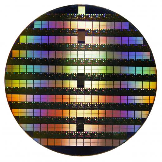
Surface micromachining is a fabrication process used to develop integrated circuits and sensors of various kinds. Using surface micromachining techniques allows applications of up to nearly 100 finely applied layers of circuit patterns on one chip. In comparison, only five or six layers are possible using standard micromachining processes. This allows many more functions and electronics to be incorporated into each chip for use in motion sensors, accelerometers that deploy airbags in a vehicle crash, or for use in navigation system gyroscopes. Surface micromachining uses select materials and both wet and dry etching processes to form the circuitry layers.
Circuitry parts made using this method were initially used in accelerometers, which deployed airbags in vehicles at the time of a crash. Surface micromachined sensors in vehicles also provide protection against roll-overs via tilt control, and are used in anti-lock braking systems. This circuitry is also in use in high-performance gyroscopes in guidance control systems and navigation systems. As circuitry produced using this method produces tiny and precise circuitry, it is possible to combine multiple functions on one chip for uses in motion sensing, flow sensing, and in some consumer electronics. In photography, when filming with a video camera, these chips give image stabilization during movement.

The surface micromachining process uses either crystal silicon chip substrates as a foundation upon which to build layers, or can be started on cheaper glass or plastic substrates. Usually, the first layer is of silicon oxide, an insulator, which is etched to a desired thickness. Over this layer, a photosensitive film layer is applied, and ultraviolet (UV) light is applied through the circuit pattern overlay. Next, this wafer is developed, rinsed, and baked for the following etching process. This process is repeated multiple times to apply more layers, with careful monitoring and precise etching techniques applied to each layer, to produce the final layered chip design.
The actual surface micromachining process of etching is done by one or a combination of several machining processes. Wet etching is done using hydrofluoric acids to etch out circuit designs on layers, cutting through unprotected insulating materials; un-etched areas of that layer are then electrolyzed to isolate the layer from the next one applied. Dry etching can be done alone, or in combination with chemical etching, using an ionized gas to bombard the areas to be etched. Manufacturers use dry plasma etching when a large portion of the layer is to be etched in a circuit design. Additionally, another plasma combination of chlorine with fluorine gas can produce deep vertical cuts through the film masking materials of a layer, as is often needed when producing microactuator sensor chips.
AS FEATURED ON:
AS FEATURED ON:


Discuss this Article
Post your comments